Waveguides Optical amplifier, Optical switch, Optical cross-connect, LIDAR system, Micromirror, Lenses, Photonics crystal

Bio/Chemical Sensing, Cantilevers, GPS, Micro-arrays, µ traps, Actuators, Microwell Biochips, Valveless micropump.

Microfludic channels design for future fast viruses diagnostics and healthcare applications systems, microwells, flow cell devices, microchip electrophoresis and drugs delivery
Bonding, Cavities Assembly, Fan-Out Wafer level Packaging (FOWLP), Chip on Substrate (CoS), Chip on Wafer (CoW), design of multi-layer build up.

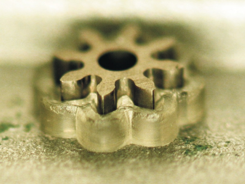
3D conducting Ag/SU-8 Microgripper design using proton beam lithography, Laser micropattering.

Display types LED, EPD, OLED and LCD and as display for e-papers, smart cards,

VCSEL’s , LED’s, Nanoscale waveguides, coupler for light coupling from fiber/Light-emitting diode (LED).

Microprocess technology, such as photoresist, is supporting advancement in the electronics field.


Gersteltec offers ready-to-use formulated products that offer extremely high transparency in the visible wavelength range for optical transmission with high mechanical, physical, thermal resistance and very good adhesion properties to various substrate materials.

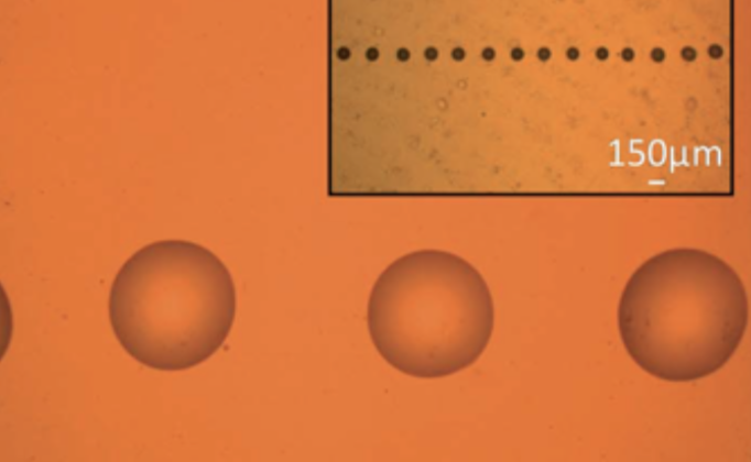
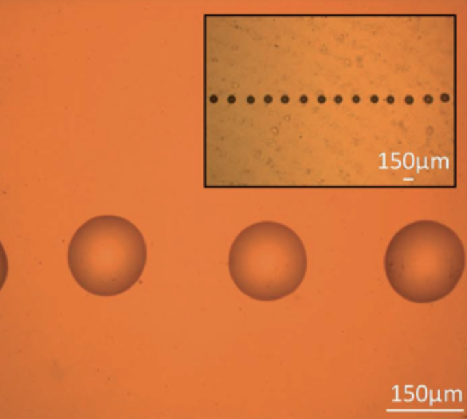
SU-8 offers the realization of monolithic auto-assembled channels for microfluidic applications, high aspect ratios micro-channels.


Gersteltec offers ready-to-use formulated products without toxicity, the workspace is transparent that is subtitle to the design of the multi-electrode array and neural applications


Gersteltec SU8 is well suited for LIGA processing. its excellent sensitivity and achievable vertical side wall profile for high precision fabrication of micro compoments by X-ray and UV light. Photoresist resist products are available in 250ml, 500ml, 1 Liter, 4 Liter bottles, in addition we can package into 10 and 20 Liter Nowpaks.


Gersteltec offers ready-to-use formulated products without toxicity for microfluidic channels, and neural applications


At Gersteltec, the smallest particles have a big effect: Gersteltec uses nano-objects to develop and produce innovative high-technology additives that give completely new combinations of properties to a wide range of epoxy substances. The results are materials with superior characteristics that give our clients a decisive lead over the competition.


Gersteltec offers ready-to-use high performance SML/SU-8 resist
Nanomaterials have unique properties which enables their utilization in functionl coating snd printing. Gersteltec research is. focused on developing Ready-to-use resist formulations of nanomaterials in a variety of viscosities and utilization of. these materials as “ink” and “paint” for customers requirements to reduced material waste. Providing ink polymers solution for drop-on-demand and micro-dispensing devices. Gersteltec developed an inkjettable low-stress dielectric with low residual stress.


Gersteltec offers ready-to-use formulated products for stamp fabrication with low cost efficient alternative to Si, quarts stamps

Gersteltec offers its customers solutions to their Display requirements by providing a combination of consulting services, application development of high transparency products with high aspect ratio resolutions an be transparent or black for pixels applications design.


Gersteltec offers ready-to-use formulated products. Customers can select filler types according to their choice. Several common fillers are used to get the desired end products that offer extremely high mechanical, physical and thermal resistance.

Gersteltec offers its customers solutions to their 3D requirements by providing SU-8 with nanoparticales of silver or silica


Gersteltec offers ready-to-use formulated products. Customers can select filler types according to their choice. Several common fillers are used to get the desired end products that offer extremely high mechanical, physical and thermal resistance.


Specifically designed for wafer-fused VCSEL technology. Lenses deposition by Drop-on Demend Inkjet processes for VCSE’ls and Micro LED devices.

Gersteltec offers coating solutions by spray to offering a combination of tailor-made nano-composites Polymer /Epoxydevelopment with a consulting service.
Gersteltec offers ready-to-use formulated products. Customers can select filler types according to their choice. Several common fillers are used to get the desired end products that offer extremely high mechanical, physical and thermal resistance.

Gersteltec offers high pur photoresist for semiconductors as vias design, low stress dielectric, spacer design for laser technology.
Gersteltec offers ready-to-use high pur formulated products for semiconductors applications